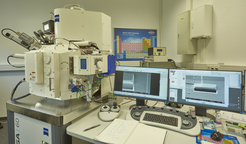
Electron Microscopy
Scanning electron microscopy allows higher resolution as well as a higher focal depth than optical microscopy by employing a high energy electron beam, which scans the sample. By detecting the secondary electrons and backscattered electrons produced at the sample surface, imaging of properties like topography, material distribution (light/heavy atoms, atomic number contrast) and micro structure (grain orientation contrast) is possible. Beyond these possibilities additional analysis tools like energy dispersive X-ray spectroscopy (EDX) and electron backscatter diffraction yield information on chemical composition and crystal orientation on a microscopic scale.

For an in-situ preparation targeted at microscopically small structures on the sample a focused ion beam is employed for coating, cutting, and polishing. This allows the preparation of cross sections of several 10 micrometres of depth. An images sequence from a series of such densely cut cross sections allows the reconstruction of three-dimensional structures. The focused ion beam also facilitates the microscopically targeted preparation and separation of microscopic material samples (<< 100 µm), like for instance thin lamellae for transmission electron microscopy ((S)TEM).